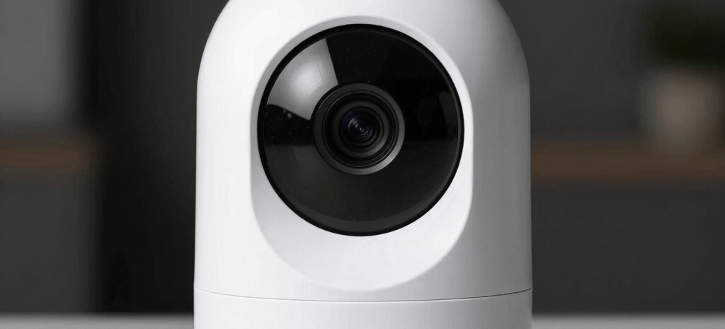
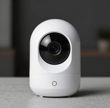
Build Smarter Cameras
How to cut costs by 27% to reach mass production in 4 months
4/8/2026
Build Smarter Camera: How to cut costs by 27% to reach mass production in 4 months
Building an AI-powered smart camera is notoriously difficult. You are cramming high-end optics, a heat-generating NPU (Neural Processing Unit), and wireless connectivity into a tiny, weather-proof enclosure.
Most Western hardware startups take 9 - 12 months to go from EVT to Mass Production (MP), and they usually miss their target BOM cost by 20%.
Here is how we reverse that trend. By leveraging the deep Shenzhen supply chain infrastructure, here is the blueprint to build a smarter camera, cut the BOM by 27%, and ship in 120 days.
Step 1: The 27% BOM Surgery (Component Localization)
Cost reduction doesn't come from beating down the factory's assembly fee. It comes from attacking the BOM.
When Western engineers design a PCBA, they default to familiar distributors (DigiKey/Mouser) and Tier-1 western silicon (TI, NXP, STMicroelectronics). In China, this is a massive cost disadvantage.
To save 27%, you must use Strategic Component Localization (Domestic Replacements):
Keep the Core: Keep your core AI SoC (e.g., Ambarella, Qualcomm, or Rockchip) and your primary image sensor (Sony or OmniVision). Do not compromise the brain or the eyes.
Localize the Peripherals: Swap the PMICs (Power Management), LDOs, flash memory, and basic microcontrollers with Chinese domestic equivalents (e.g., GigaDevice, Silergy, or SG Micro). These components are pin-to-pin compatible, offer identical performance, and are often 40% to 60% cheaper with zero lead-time issues.
Direct Lens Sourcing: Stop buying off-the-shelf optical modules from western catalogs. Go directly to the Tier-2 optical assembly houses in Dongguan. You can get custom-tuned multi-element glass/plastic lenses at a fraction of the cost.
Step 2: DFM for Optics & Thermals (Preventing Delays)
You cannot hit a 4-month timeline if you have to re-cut steel tooling because the camera overheats or loses focus.
Smart cameras have two mortal enemies: Heat and Optical Misalignment. Before cutting any tooling, your on-the-ground engineering team must execute a ruthless DFM (Design for Manufacturability) audit.
Thermal Dissipation DFM: AI chips run hot. If the plastic enclosure traps heat, the sensor generates noise. DFM must ensure the PCB is properly coupled with thermal gap pads directly to a die-cast aluminum heat sink or chassis.
Active Alignment (AA) vs. Threaded Focus: If you are building a high-res AI camera, manual threaded lens focusing on the assembly line will ruin your yield rate. Design the PCBA and lens holder for Active Alignment (AA) equipment. The factory machine actively powers on the sensor, measures the MTF (sharpness) in real-time, and uses UV glue to freeze the lens in the perfect micron-level position. This increases upfront NRE but slashes assembly time and scrap rates.
Step 3: The 120-Day "Async" Execution Sprint
How do you compress 9 months into 4? You stop shipping prototypes across the Pacific Ocean.
Traditional timeline: Factory makes a sample -> ships to California (1 week) -> US team tests it -> emails feedback -> factory updates. This sequential loop kills startups.
By utilizing the Async Advantage (having ex-DJI/Huawei engineers on the ground in Shenzhen), the timeline compresses:
Month 1: EVT & DFM Lock.
BOM optimization is finalized. PCBA is spun locally in 5 days.
Soft tooling (aluminum/silicone) is used to verify mechanicals.
Month 2: DVT & Hard Tooling.
Steel is cut for injection molding.
The Cheat Code: When T1 (first tool) plastic parts come off the press, your Shenzhen engineering team is standing next to the machine. They measure the tolerances with calipers immediately, approve the T2 modifications on the spot, and shoot a Loom video to the US founders. Time saved: 3 weeks of shipping.
Month 3: PVT (Production Validation) & Certs.
Run 200 units on the actual assembly line to train the operators.
Establish the SOPs, the optical testing darkrooms, and the IP67 waterproofing leak-test stations.
Month 4: Mass Production (MP).
Ramp up. Live video feeds of the assembly line are sent to the US team.
Outbound Quality Control (OQC) clears the shipment.
Step 4: The IP Shield (Black-Box Assembly)
You want the cost savings of China, but you don't want your smart camera cloned on AliExpress next month.
If you hand your complete CAD, firmware, and BOM to a single factory, you are taking a massive risk. To build safely, you must deploy a Split-BOM & Assembly Separation Strategy:
Legal Framework: Operate entirely under Hong Kong Common Law. NDAs and manufacturing contracts are executed via a Hong Kong entity, making them internationally enforceable.
Component Decoupling: Factory A produces the die-cast housings. Factory B does the PCBA SMT. The lens modules come from Factory C.
Final Assembly: No single factory sees the whole picture until Final Assembly, Test, and Pack (FATP), which is overseen by your dedicated, trusted engineering project manager. Firmware is flashed securely via locked test jigs, ensuring the factory never has access to the raw source code.
The Bottom Line: Infrastructure over Middlemen
Achieving a 27% cost down in 4 months is not a miracle; it is a highly systematic process. However, it cannot be achieved by a US team trying to manage a traditional "sourcing agent" via midnight WeChat calls.
It requires Engineering Infrastructure.
Email Us
Flat 2401, Industrial Building, San Po Kong, Hong Kong 999077