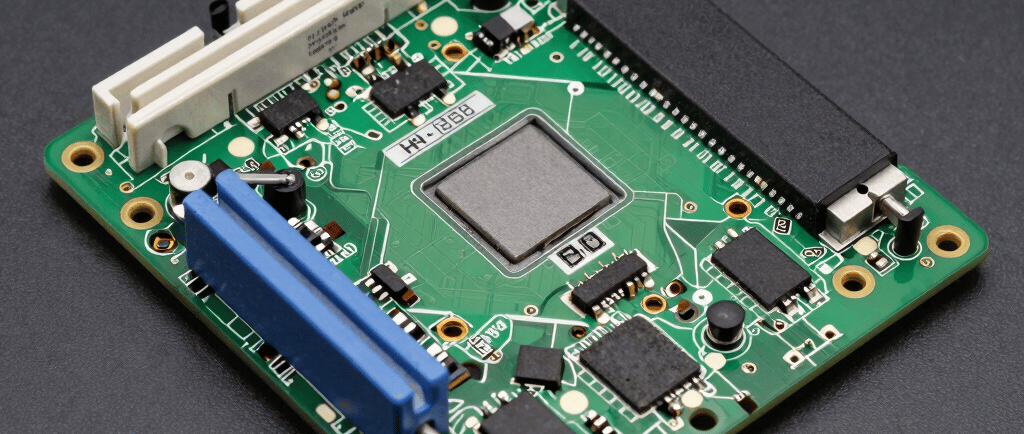
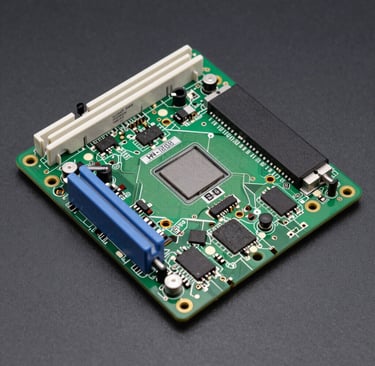
In the highly competitive semiconductor and smart hardware industry, the Printed Circuit Board Assembly (PCBA) - specifically complex boards like Motherboards housing CPU sockets and GPU PCIe slots—represents the beating heart of our products. It also represents one of our most complex cost centers.
As hardware profit margins tighten, traditional BOM (Bill of Materials) costing is no longer sufficient. We must adopt an advanced Total Cost of Ownership (TCO) Model. To effectively manage costs, we must first deeply understand the manufacturing process, deconstruct it granularly, and apply algorithmic cost drivers to every single element of the Cost of Goods Sold (COGS).
Here is a detailed breakdown of the standard Motherboard PCBA manufacturing process and how we build a comprehensive Cost Model around it to drive profitability.
Part 1: Deconstructing the PCBA Manufacturing Process
Based on standard industry practice for complex motherboards, the manufacturing journey is highly sequenced, transitioning from automated high-tech placement to manual assembly and rigorous testing. We break this down into 7 distinct stages:
1. Material Preparation (The Foundation)
Before assembly begins, rigorous material handling is required.
IQA (Incoming Quality Assurance): Inspecting raw components.
MSD (Moisture Sensitive Devices) Management: Baking and sealing sensitive chips to prevent "popcorning" during soldering.
Automated Reel Sorting: Organizing component reels for efficient machine loading.
2. SMT (Surface Mount Technology) - Highly Automated
This is where the majority of tiny components are placed onto the bare PCB.
Solder Paste Printing: Applying conductive paste through a stencil.
High-Speed Placement (Pick-and-Place): Rapidly mounting small resistors/capacitors.
Chipset Placement: Precision mounting of large ICs (Integrated Circuits).
Reflow Soldering: Passing the board through an oven to melt the paste and secure components.
AOI (Automatic Optical Inspection): Camera systems checking for missing or misaligned parts.
3. PCB Edge Processing
Routing/Milling: Removing scrap board material and separating panels into individual motherboards.
4. DIP (Dual In-line Package / Through-Hole Technology)
Used for components that SMT machines cannot handle (e.g., large Capacitors, PCIe slots, I/O ports) which require pins to go through the PCB.
Auto Insertion: Machines rapidly inserting standard through-hole parts (e.g., at a rate of 0.8 seconds/piece).
Manual Insertion: Human operators placing non-standard or bulky connectors.
Wave Soldering: Passing the bottom of the board over a wave of liquid solder to secure the through-hole pins.
Cooling & Secondary AOI: Cooling the board and inspecting the wave solder joints.
5. Cleaning & Testing
Automatic Plate Brushing/Cleaning: Removing flux residue to ensure long-term reliability.
ICT (In-Circuit Test) / Flying Probe Test: Electrically probing the board to find short circuits or dead components.
6. Assembly & Function Test
CPU Socket ILM Assembly: Installing the intricate mechanical retention mechanism for the CPU.
Heatsink Assembly: Mounting thermal armor and cooling blocks.
Function Testing (Circuit): Powering on the board to simulate real-world operation.
7. Packaging & Logistics
Anti-static Bagging: Protecting the board from ESD (Electrostatic Discharge).
Box Folding & Accessories: Adding manuals, cables, and final boxing.
Weighing: A final quality check to ensure no accessories were missed before shipping.
Part 2: The Comprehensive Motherboard Cost Model
To understand the pricing logic of electronic hardware, we must build a granular manufacturing cost model based on the processes outlined above. If we take a standard high-end motherboard with a target retail price of $250, the structural breakdown of the COGS and associated expenses looks like this:
1. BOM Cost (Bill of Materials) - Approx. 60% - 70%
This represents the physical hardware and is our largest expenditure:
Core Silicon: The Z890 or X670 chipset purchased from Intel/AMD (typically the single most expensive component).
Bare PCB: High-frequency, 6-layer or 8-layer fiberglass copper-clad laminates.
VRM Power Delivery: DrMOS, chokes, and solid capacitors. As power phases increase for overclocking, this cost scales linearly.
Connectors: High-cost mechanical parts like the LGA 1851 CPU socket, SMT-reinforced PCIe slots, DDR5 slots, and high-speed USB/Type-C arrays.
Controllers: Realtek/Intel LAN chips, Wi-Fi modules, and dedicated audio DACs.
Mechanical & Thermal: Heavy extruded aluminum VRM armor, copper heat pipes, M.2 toolless latches, and screws.
2. MVA Cost (Manufacturing Value Added) - Approx. 10% - 15%
MVA encapsulates all the "factory activities" (Steps 1 through 7) required to turn the BOM into a finished product:
Direct Labor: Wages for assembly line workers performing manual DIP insertion, screw driving, and functional testing.
Machine Depreciation & Consumables: Amortization of multi-million-dollar Fuji SMT placement machines, reflow ovens, and wave soldering equipment. This also captures vital consumables like solder paste, flux, and nitrogen gas used in soldering.
Factory Overhead: Rent for the facility (e.g., in Shenzhen), industrial electricity, cleanroom anti-static apparel, and warehousing maintenance.
3. Testing & Yield Loss (Scrap Rate) - Approx. 3% - 5%
Quality is not free, but it is cheaper than failure:
Yield Loss: Manufacturing is never 100% perfect. A percentage of boards will be irrevocably damaged during SMT or DIP. The sunk cost of these scrapped boards must be amortized and added to the cost of the "good" boards.
Testing Costs: Electricity for AOI machines, labor time for ICT, functional "power-on" testing, and the ongoing wear-and-tear of test fixtures.
4. Packaging & Logistics - Approx. 5%
The cost to protect and move the product (Step 7):
Packaging Materials: Full-color retail boxes, premium anti-static bags, manuals, and aesthetic stickers.
Logistics & Tariffs: Freight costs (ocean or air freight from the Asian factory to global distribution hubs) and import duties.
5. R&D, SG&A & Margin - Approx. 10% - 15%
The remainder dictates our business viability:
NRE (Non-Recurring Engineering): Amortizing the salaries of PCB layout engineers and the BIOS/firmware development teams.
SG&A (Marketing): Advertising budgets and sponsorships for tech influencers and reviewers.
Manufacturer Margin: Hardware manufacturing operates on notoriously thin margins. Leaving 10% to 20% for the manufacturer requires strict reliance on high sales volume to generate absolute profit.
Part 3: TCO Management – Moving Beyond the Factory Gate
As a Senior Cost Manager, I emphasize that understanding this structural breakdown allows us to manage the Total Cost of Ownership (TCO), focusing particularly on Field Costs (warranty and aftermarket failures).
1. The ROI of Testing (MVA vs. Field Cost)
Cost engineers often face pressure to speed up the line by reducing testing times (cutting MVA costs). Our TCO model proves this is a false economy. Finding a bad solder joint at SMT AOI costs cents. Finding it in the field (a dead motherboard in a customer's PC) costs hundreds of dollars in RMA (Return Material Authorization) logistics and brand damage. The investment in Step 5 (Testing) is mathematically justified by the asymmetric reduction in Field Costs.
2. Design-to-Cost (DTC) Optimization
By analyzing the granular breakdown of our BOM vs. MVA, we identify trade-offs. Wave Soldering (DIP) adds significant labor and energy overhead. If R&D can replace a through-hole capacitor with a surface-mount equivalent, we shift components from DIP to SMT. This reduces cycle time and manual labor (lowering MVA), even if the SMT component is slightly pricier on the BOM, resulting in a lower Total Ex-Factory Cost.
In smart hardware, managing PCBA costs requires far more than sheer intuition or beating up suppliers on silicon prices. By scientifically deconstructing the manufacturing process and feeding it into a dynamic, granular Cost Model that tracks BOM, MVA, Scrap, and Logistics, we unlock the ability to make strategic decisions. This is how we protect our thin margins, invest intelligently in quality, and secure long-term profitability in the 0-to-1 hardware journey.